
How CPUs Execute Instructions
A Deep Dive into the Fetch Decode Execute Cycle

“I like to understand how things work at the lowest level because that is where the real control lies” – Unknown”
When I first traced how instructions flow through a CPU, the “magic” of software quickly disappeared. It became clear that computing is actually just a precise system of electrical signals and logic gates.
Every modern processor executes billions of these simple operations per second. For a developer, understanding this mechanical process is practical. It gives you an edge in performance tuning and debugging low-level issues.
The core mechanism driving this is the Fetch-Decode-Execute cycle, but to understand how it works, we first need to look at the hardware components inside.
The CPU
The CPU is the primary component responsible for interpreting and executing instructions from the computer’s memory. Rather than acting autonomously, it operates strictly within the bounds of a defined Instruction Set Architecture (ISA), manipulating data via low-level primitives.
Instruction Set Architecture is the fundamental interface between software and hardware defining CPU instructions, data types, registers, I/O models, and operations. It is an abstract model defining how software controls a computer’s processor. It is important because it allows the same software to run on different processors (e.g., Intel, AMD) that implement the same ISA.
These binary instructions trigger specific hardware sequences to.
Transfer Data. Move values between registers and memory (Load/Store).
Compute. Utilize the Arithmetic Logic Unit (ALU) for mathematical and bitwise operations.
Control Flow. Alter the execution path via branch or jump instructions based on flag states.
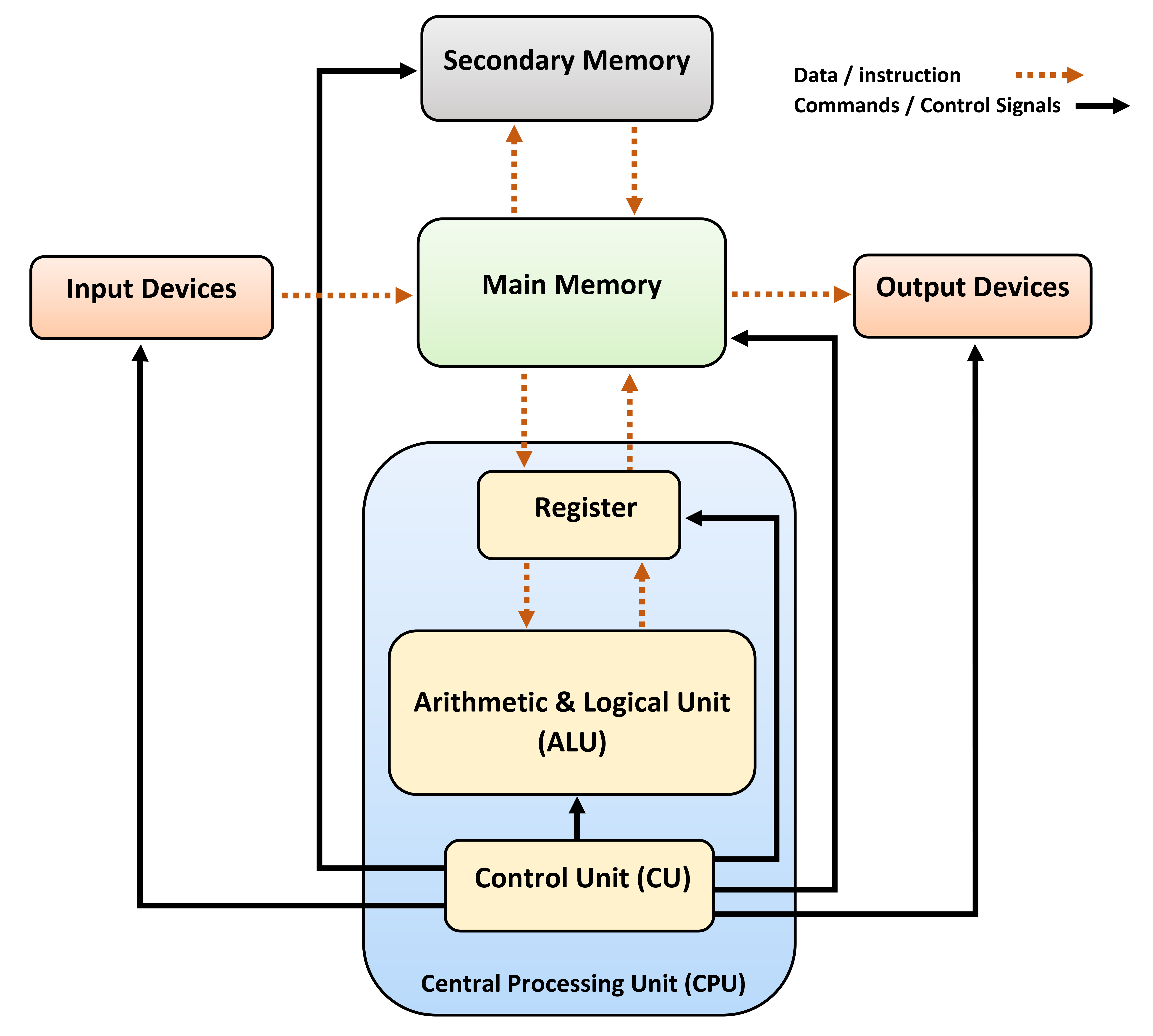
The CPU’s operation is driven by the Fetch-Decode-Execute cycle, clocked by an oscillator to ensure synchronization across logic gates.
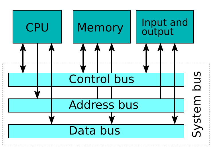
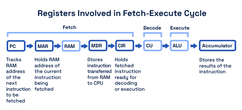
The fetch-decode-execute cycle (or instruction cycle) is the fundamental process a CPU uses to run programs, involving three main steps. Fetch (getting an instruction from memory), Decode (translating the instruction into commands), and Execute (carrying out the action, like math or data movement). This cycle repeats continuously, driven by the system clock, allowing computers to process billions of instructions per second by moving data between RAM and CPU registers, using buses (address, data, control).
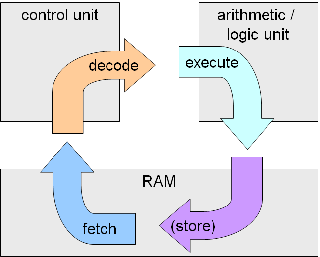
Step One. Fetch = Grabbing The Instruction
The fetch stage initiates the instruction cycle by retrieving the opcode and operands from memory. This process is governed by the system clock and involves coordinated data movement between specific CPU registers and the memory interface.
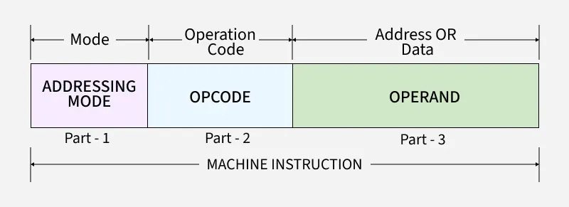
The opcode (operation code) is the crucial part of a machine instruction that tells the processor what operation to perform (like ADD, MOVE, LOAD). During the fetch stage, the CPU retrieves this binary opcode from memory, then uses it in the decode stage to activate the correct hardware (ALU, registers) for the specified task, identifying the data (operands) needed from the instruction.
1. Address Generation
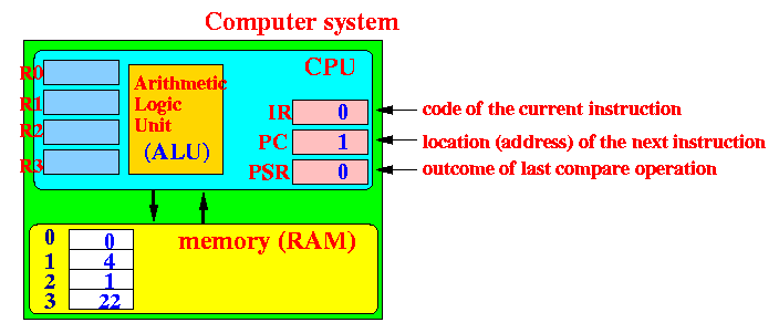
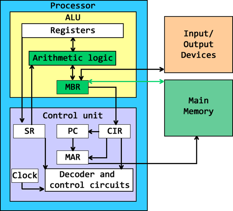
The Program Counter (PC) holds the memory address of the next instruction. To initiate a fetch, the CPU copies the PC’s value to the Memory Address Register (MAR) via the internal bus (MAR ← PC). The Control Unit then asserts a READ signal on the control bus and places the address onto the system address bus.
2. Instruction Retrieval & Caching
While logically retrieving from “main memory,” modern architectures prioritize the L1 Instruction Cache (I-Cache).
Cache Hit. If the requested address is present in the L1 I-Cache (low latency), the instruction is immediately available.
Cache Miss. The request propagates down the memory hierarchy (L2, L3, RAM), incurring significant latency cycles (wait states).

3. Data Transfer
The fetched binary data returns via the data bus to the Memory Buffer Register (MBR) (also known as the MDR), and is finally copied to the Instruction Register (IR) (IR ← MBR).
4. Program Counter Update & Prefetching
Simultaneously, the PC is incremented to point to the next sequential address (PC ← PC + instruction_length). To minimize pipeline stalls, the Branch Prediction Unit (BPU) may speculatively trigger the prefetcher to load instructions from non-sequential addresses before the current instruction is even decoded, relying on history tables to predict branch targets.
Fetch. The Control Unit (CU) retrieves the next instruction from the memory address stored in the Program Counter (PC) and loads it into the Instruction Register (IR). The PC is then incremented.
Step Two. Decode = Understanding the Instruction
Once the binary instruction is loaded into the Instruction Register (IR), the CPU needs to figure out what to do with it. This is the job of the Control Unit. It breaks the binary sequence down into two primary components:
Opcode (Operation Code). The specific action to perform (e.g.,
ADD,LOAD,JUMP).Operands. The data or locations required for the action (e.g., a specific register ID, a memory address, or a raw number).
Generating Control Signals
The Control Unit effectively acts as a switchboard. Based on the opcode, it asserts specific electrical control signals that traverse the rest of the processor. These signals orchestrate the flow of data by:
Opening or closing logic gates (multiplexers) to route data between registers.
Signaling the ALU to select a specific mathematical function.
Enabling read or write lines to main memory.
Micro-operations (μops)
In simpler architectures (like early RISC), instructions are executed directly. However, in complex modern CPUs (like x86), a single “macro” instruction (like writing a string to memory) is often too complex to execute in one go.
To handle this, the decoder translates the single instruction into a sequence of smaller, primitive internal commands called micro-operations (or μops). This allows the processor to break down complex tasks into manageable steps that can flow smoothly through the pipeline.
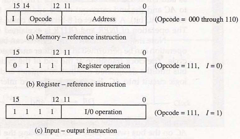
Decode. The Control Unit (CU) interprets the binary code in the Current Instruction Register (CIR). It identifies the operation (e.g., ADD, LOAD) and any required data/operands. Control signals are generated to activate the necessary CPU components (registers, ALU).
Note: Opcodes are used to identify the specific operation the CPU must perform.
Step Three. Execute = Performing the Operation
During this stage, the control signals generated during decoding activate specific functional units within the CPU to perform the operation.
Arithmetic & Logic. The ALU (Arithmetic Logic Unit) handles integer math (
ADD,SUB) and bitwise operations (AND,XOR). Floating-point calculations are often offloaded to a specialized FPU.Memory Access. For
LOADorSTOREinstructions, the CPU calculates the effective memory address. The Load/Store Unit then manages the transfer of data between registers and the cache or RAM.Control Flow. Branch instructions evaluate specific condition flags (like Zero or Overflow). If a condition is met, the Program Counter is updated to a new address, altering the execution path.
Modern Optimizations
Execution creates the most significant bottlenecks, so modern architectures mitigate latency using two key techniques:
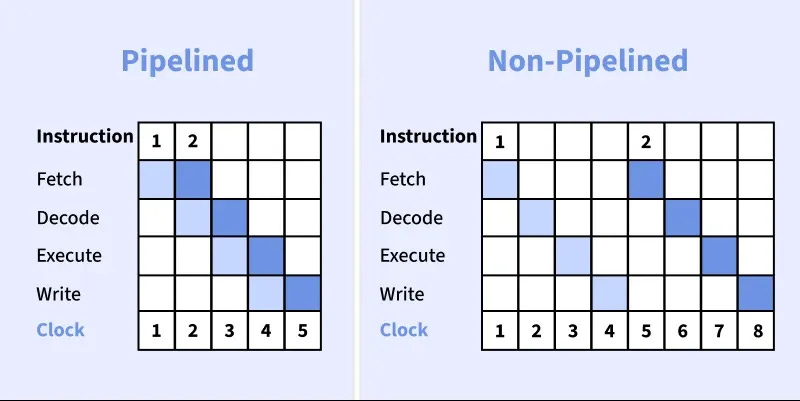
Pipelining. Like an assembly line, the CPU overlaps stages. While one instruction is executing, the next is being decoded, and the third is being fetched.
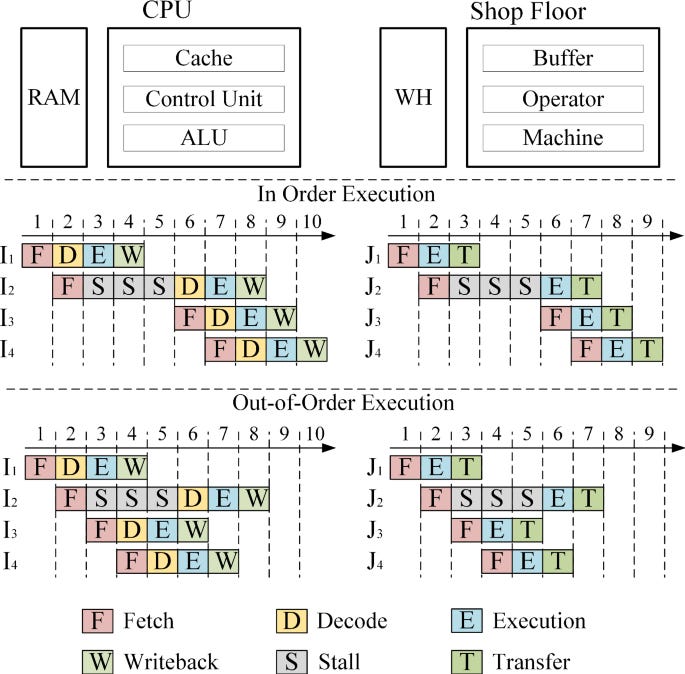
Out-of-Order Execution (OoO). Instead of waiting for a slow instruction (like a memory fetch) to finish, the scheduler identifies independent instructions and executes them ahead of time, reordering the results later to maintain program correctness.
Execute. The CPU performs the operation. This may involve the ALU calculating a result, the CU asserting read/write signals to memory, or updating specific registers (like the Accumulator or Stack Pointer).
Step Four. Repeat and Continuity
The final phase of the cycle ensures the system state is consistent for the next operation.
Writeback. Results from the execution stage are written back to a destination—usually a register or a memory address.
Cycle Repeat. The Program Counter (PC) is updated to point to the next instruction address.
This loop is the heartbeat of computing. While conceptually simple, modern processors execute this cycle at rates exceeding 3–5 GHz (billions of cycles per second). The challenge is not just execution speed, but coordinating the data flow so the CPU never idles.
Core CPU Components in Depth
To sustain this throughput, the CPU relies on a set of specialized hardware units.
Registers. The fastest tier of storage in the computer. These are ultra-low latency locations directly on the CPU die.
General Purpose Registers (GPRs). Store operands and intermediate results.
Special Purpose Registers. Include the Program Counter (PC), Instruction Register (IR), and Status Flags (which track overflow, zero results, etc.).
Arithmetic Logic Unit (ALU). The combinational logic circuit responsible for all integer arithmetic (
ADD,SUB) and bitwise operations (AND,NOT,XOR).Control Unit (CU). The coordinator. It decodes instructions and manages the “traffic signals” (control lines) that open/close gates between registers, the ALU, and system buses.
Memory Hierarchy. To prevent the fast CPU from waiting on slow system RAM, modern architectures use multi-level caches (L1, L2, L3). These stores frequently accessed data closer to the execution units.
CPU is so cool to learn about!!!